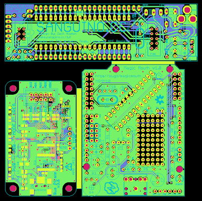
FusionPCB offer a fabulous PCB prototyping service — 10 boards each 10 x 10 cm for just $25 plus postage. The Magic Mouth v1.0 Arduino speech shield occupies 5.3 x 6.9 cm leaving plenty of space for other panels. But the freeware version of Eagle that I use imposes maximum dimensions of 8 x 10 cm, and I would like to use all the space available. For example, the picture above shows the shield next to a Bus Pirate v3.6 PCB and below a (slightly squeezed) Sanguino. This layout uses the full 10 cm in each dimension.
So this evening I hacked together a short Perl script that merges 2 sets of Gerber files together. To use the script, type:
perl GerberMerger.pl prefixA prefixB Xoffset Yoffset
where prefixA is the name of the first set of Gerber files, prefixB is the name of the second set of Gerber files, and the Cartesian offset between the two sets of files is specified by (Xoffset, Yoffset). I don't claim that it works for every Gerber file in existence. All I know is that it works for Gerbers generated from Eagle by the FusionPCB CAM file using the freeware Gerber viewer gerbv and Perl version 5.14.2.
Please note that FusionPCB require that the "board outline must be included at least in one layer". This means that it is not enough to panelize the PCBs by merging the Gerbers, it is also necessary to draw an outline around the panelized boards somehow. One way is to copy and paste the "Dimension" layers from all the panels into your PCB design software, arrange them however you like, and use these outlines as a template when merging. After running the CAM job the outline will be contained in the .GML file and should be submitted along with the other Gerbers.
No doubt there exists far more sophisticated software out there, but this seems to do the job for me.
Update: Here are the manufactured boards from FusionPCB. With a 1 mm solder masked gap between the boards they were very easy to depanelize.


1 comment:
cool...thanks. I'll have to give this a try :-)
Post a Comment